High-speed Interface
High-speed Interface
With the emergence of various applications such as AI, IoT, and 5G wireless systems, the demand for higher data-bandwidth memories has increased. Therefore, higher data-rate per pin is needed in high-speed interfaces. The techniques to achieve higher data-rate are as follows:
- Equalization
- Multi-level signaling
- ZQ calibration
Equalization(1/2)
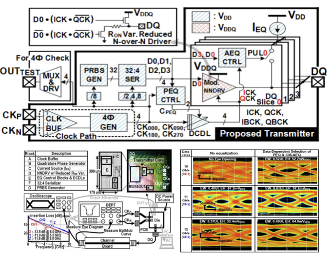
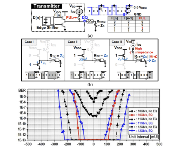
As the data-rate per pin increases, so does the channel loss, which causes signal integrity (S/I) degradation. Equalization technique is needed to prevent such S/I degradation, however, it requires extra power and area. Therefore, low-power equalization that improves S/I without significantly increasing power consumption is required. This paper presents a low-power DRAM transmitter that improves impedance matching and reduces energy consumption by alternating between phase equalization and current-mode amplitude equalization. The transmitter, implemented with a voltage-mode driver, compensates for channel loss and enhances signal integrity by minimizing on-resistance variations. A prototype chip, fabricated using a 65 nm CMOS process, successfully achieves a data rate of 12 Gb/s while maintaining low energy consumption of 1.30 pJ/bit. The design includes both amplitude and phase equalization techniques, optimized to enhance performance for DRAM interfaces. Measurements demonstrate that the proposed transmitter effectively increases the eye height and width, improving overall signal transmission quality.
S. Lee, Y.-U. Jeong, J. Yun, J.-H. Chae, and S. Kim, "A Low-Power DRAM Transmitter with Phase and Current-Mode Amplitude Equalization to Improve Impedance Matching," IEEE Transactions on Circuits and Systems-II, vol. 69, no. 11, pp.4208-4212, November 2022.
Equalization(2/2)
As the data-rate per pin increases, so does the channel loss, which causes signal integrity (S/I) degradation. Equalization technique is needed to prevent such S/I degradation, however, it requires extra power and area. Therefore, low-power equalization that improves S/I without significantly increasing power consumption is required. This paper presents a low-power DRAM transmitter that improves impedance matching and reduces energy consumption by alternating between phase equalization and current-mode amplitude equalization. The transmitter, implemented with a voltage-mode driver, compensates for channel loss and enhances signal integrity by minimizing on-resistance variations. A prototype chip, fabricated using a 65 nm CMOS process, successfully achieves a data rate of 12 Gb/s while maintaining low energy consumption of 1.30 pJ/bit. The design includes both amplitude and phase equalization techniques, optimized to enhance performance for DRAM interfaces. Measurements demonstrate that the proposed transmitter effectively increases the eye height and width, improving overall signal transmission quality.
S. Lee, Y.-U. Jeong, J. Yun, J.-H. Chae, and S. Kim, "A Low-Power DRAM Transmitter with Phase and Current-Mode Amplitude Equalization to Improve Impedance Matching," IEEE Transactions on Circuits and Systems-II, vol. 69, no. 11, pp.4208-4212, November 2022.
Multi-level Signaling
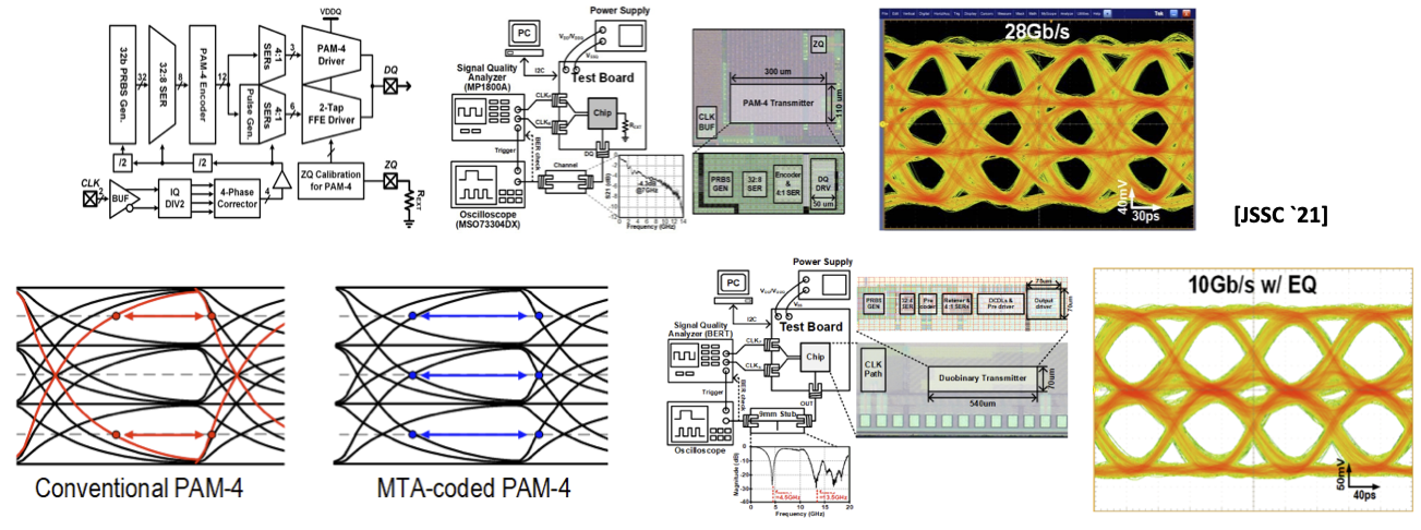
Increasing clock frequency for higher data rate leads to narrow unit interval (UI) that makes the signal more vulnerable to frequency-dependent channel loss. Since there is a limit to increasing the clock frequency with the NRZ signaling, multi-level signaling has been adopted. Unlike NRZ, multi-level signaling (PAM-3/PAM-4, etc.) is notably impacted by channel ISI and crosstalk. This has prompted diverse studies, including Duo-binary and maximum transition avoidance (MTA) coded PAM-4.
Impedance Calibration
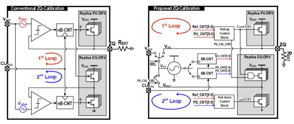
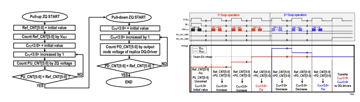
Impedance mismatch between the channel and the input/output (I/O) driver also causes the S/I degradation at high speed. Therefore, accurate impedance matching is required for better signal integrity. More precise performance was achieved compared to before with time-domain ZQ calibration.
Clock Generation & Correction
Clock Generation & Correction
Clock signals are essential for both digital and analog circuits in various applications such as memory interface and RF systems. In modern ICs, high performance clock generation and correction circuits are needed to generate signals of higher frequency and lower noise (jitter). Clock generation and correction circuits can be categorized into two fields.
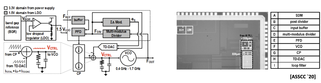
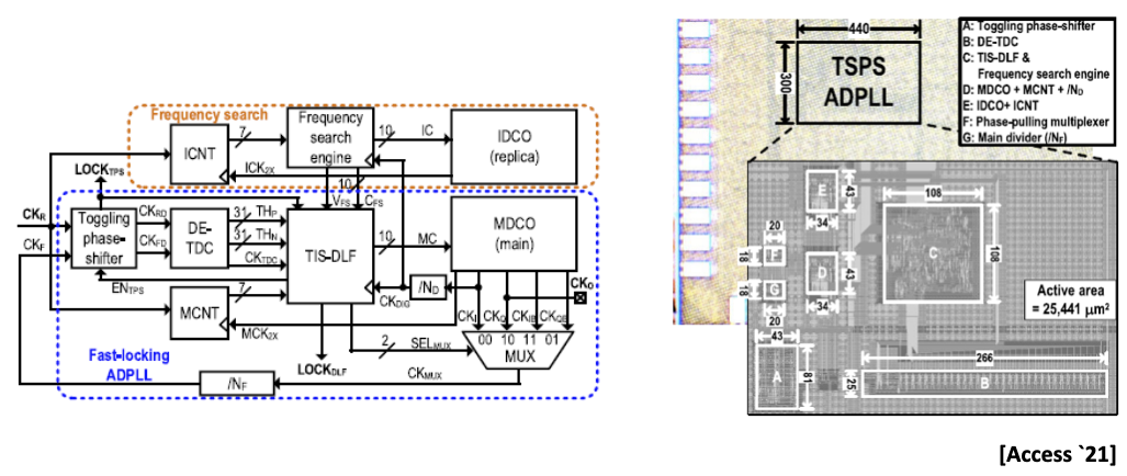
PLL (Phase Locked Loop)
PLLs are commonly used in most digital ICs for clock signal generation. A lower-frequency reference clock (from a crystal oscillator) with frequencies usually less than 100MHz is input to a PLL to generate a higher frequency signal to produce a higher frequency clock in the GHz range.
Depending on the system application, PLLs are designed to maximize performance of the following:
- Fast locking time
- Low jitter/noise
- Low power consumption
- Frequency range and resolution
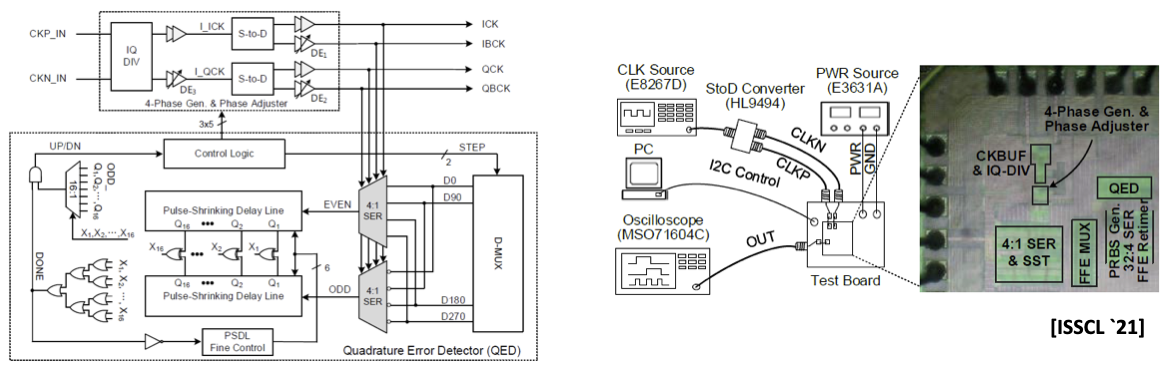
DLL (Delay Locked Loop)
DLLs are similar to PLLs, but frequency of the input and output clock signals are of the same frequency using a delay line in lieu of an oscillator. As such, DLLs are not used for frequency synthesis, but rather for deskewing.
- Deskewing – multiple clock signals (i.e., quarter-rate clocking systems) will become out of phase the further and longer they travel from the source (i.e., PLL) within a chip. Deskewing technique ensures multiple clock signals to be in-phase and be synchronously passed onto different system blocks.
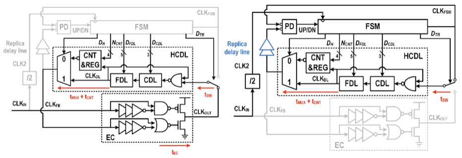
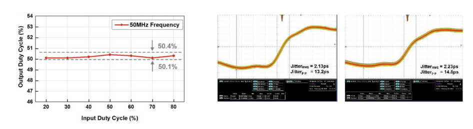
DCC (Duty-Cycle Corrector)
DCC is essential for common memory interfaces as overall performance of system is affected by the duty-cycle of the clock signal. DCC compensates duty-cycle distortion by various sources such as the process, voltage, temperature variations and device noises.
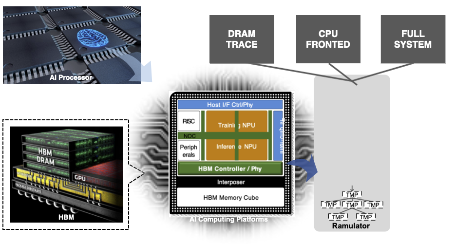
Processing-in-Memory (PIM)
PIM(Processing in Memory)
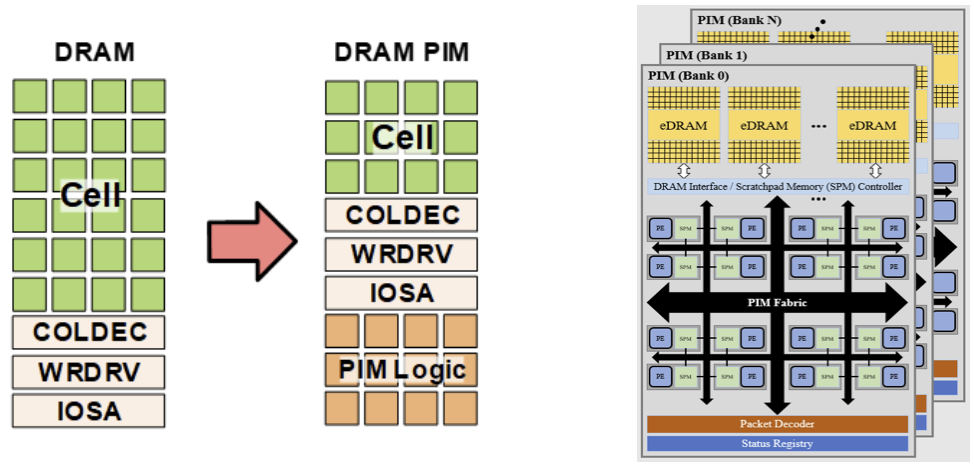
PIM(Processing in Memory) is a technique that integrates processor and memory on a single chip. This technique can enhance the speed of AI processors by reducing the travel time between CPU and memory. PIM can be applied to any application that use memory.
- Memory & Interface for eDRAM
- Implementing eDRAM
Memory & Interface for eDRAM
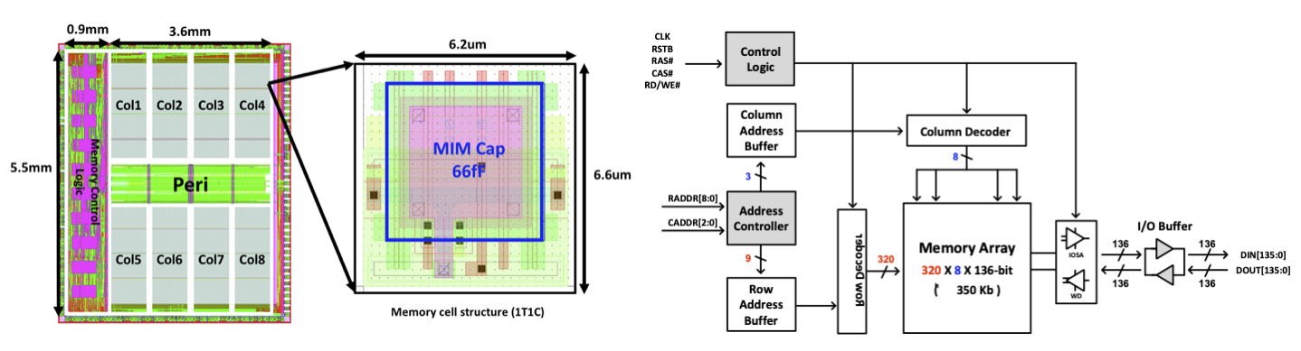
eDRAM is widely used as cache which substitutes SRAM, because it can be implemented in logic process. Our research focuses on how to improve operating speed and lower power consumption on eDRAM. Also, we design interface circuits for eDRAM and PIM.
Implementing eDRAM
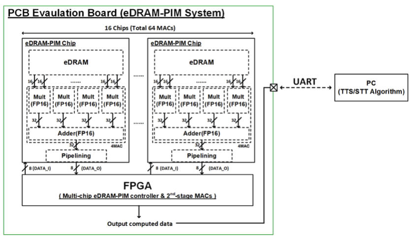
Verifying PIM functionality (Read, Write, Refresh) is very important. Our lab was responsible for verifying the eDRAM model using Verilog to ensure that it fits with the operation of real eDRAM. Additionally, we developed a chip that combines the manufactured eDRAM chip with MAC operations and designed an interface to align number of pins with the processor. This allowed us to verify the implementation of PIM at the system level.
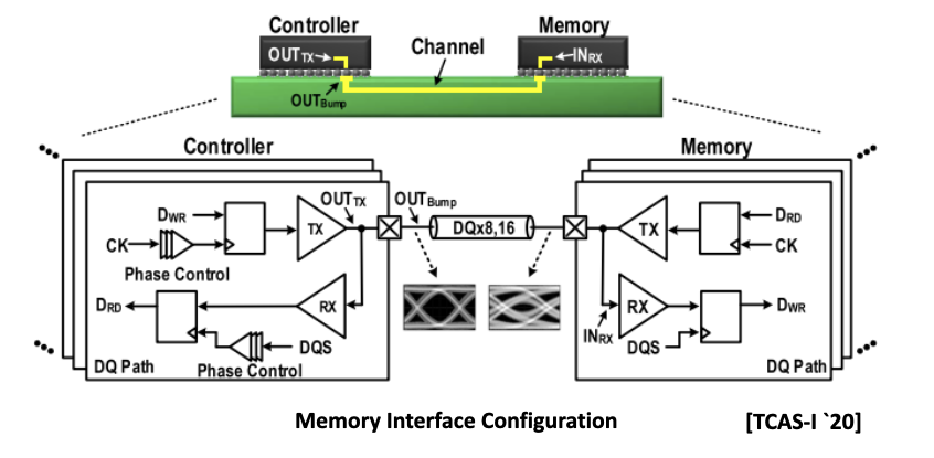
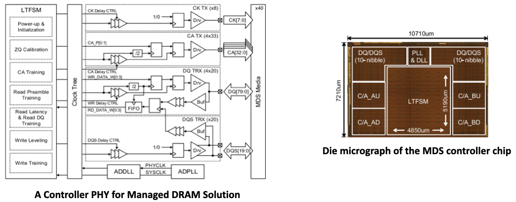
Memory & Controller PHY
Memory & Controller PHY
PHY means a physical layer that connects a link layer device with a transmission medium. In a memory interface, PHY is used to transmit and receive data between a memory device and a memory controller. PHY should be designed to satisfy each interface specification such as LPDDR and HBM. As the bandwidth of memory increases, reduced power consumption, increased data rates and improved cost-effectiveness have become important in PHY.
Next Generation HBM
Next Generation HBM Controller Physical Layer Transceiver Design
- HBM3+ and HBMx are attracting attention as accelerators and next-generation server memory due to their large capacity, wide bandwidth, and low power compared to other memories.
- In HBM3+ and HBMx, the data transmission rate per pin (>6.4 Gbps) increases, and the number of parallel I/O decreases signal integrity, resulting in bottleneck, so it is necessary to develop next-generation interface circuit technology.